
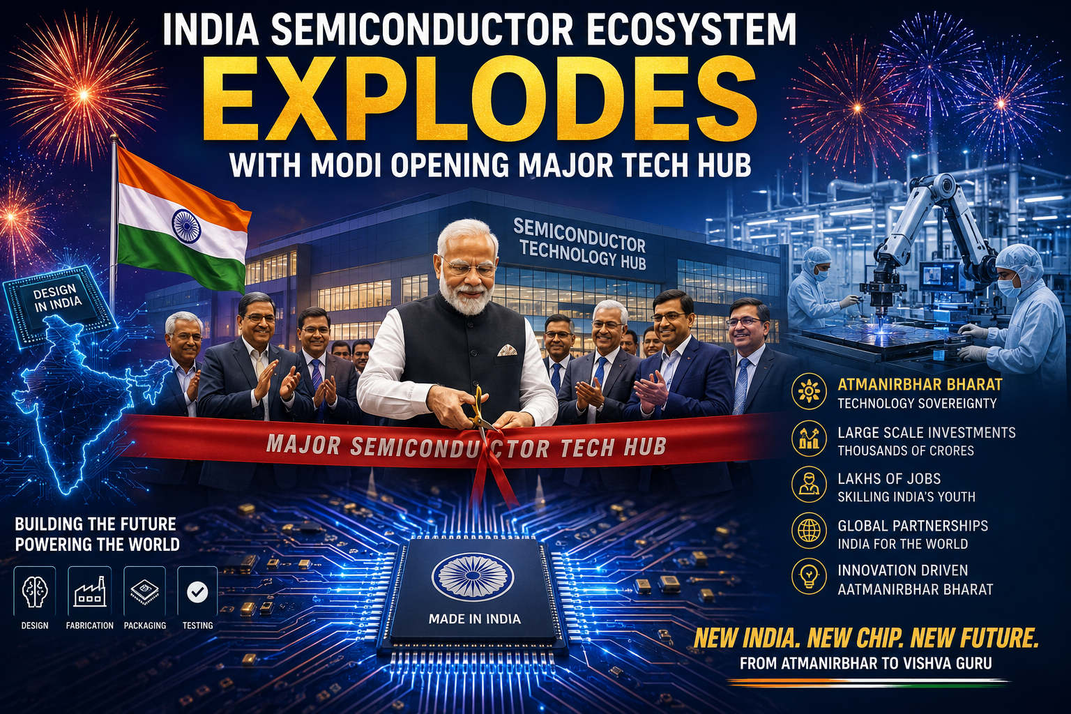
The India Semiconductor Ecosystem took a monumental leap forward as Prime Minister Narendra Modi officially inaugurated commercial chip production at the state-of-the-art CG Semi Outsourced Semiconductor Assembly and Test (OSAT) facility in Sanand, Gujarat. This landmark launch represents a critical tipping point in the nation’s technological roadmap, shifting India from a consumer of imported electronics to a dominant force in the global hardware supply chain.
Addressing a gathering of international industry captains, policymakers, and engineering professionals, Prime Minister Modi emphasized that this facility is not merely an isolated business venture, but the blueprint for a fully integrated, self-reliant technological future.
Facility Name: CG Semi Private Limited (G1 OSAT Plant)
Location: Sanand, Gujarat, India
Total Investment: ₹7,600 Crore (~$870 Million USD)
Initial Capacity: 200 Million chips annually
Target Capacity: 5 Billion chips annually (15 Million/day)
Key Partners: CG Power (92.3%), Renesas Electronics (Japan), Stars Microelectronics (Thailand)
From Foundation to Production: A Breakthrough Timeline
The launch of the CG Semi facility shatters traditional infrastructure timelines in the subcontinent. Typically, high-tech industrial installations of this magnitude require multi-year gestational periods plagued by regulatory and logistical hurdles. However, the Sanand facility transitioned from a conceptual blueprint to physical commercial manufacturing with unprecedented speed.
Prime Minister Modi had laid the foundational stone for the facility under the aegis of the India Semiconductor Mission (ISM). By late summer, the infrastructure was sufficiently advanced to initiate primary chip testing protocols. Less than a year from that testing phase, the plant has opened its gates for full-scale commercial manufacturing, ready to ship its first batches of packed microchips directly to international markets, including Japan.
This hyper-accelerated timeline underscores a deliberate paradigm shift in India’s executive execution. As the Prime Minister noted during his address, this facility stands as concrete proof that the nation no longer just conceptualizes sweeping industrial reforms but possesses the bureaucratic agility and engineering capacity to execute them on schedule.
Strategic Significance of the CG Semi Venture
The CG Semi plant operates as an Outsourced Semiconductor Assembly and Test (OSAT) hub. In the broader architecture of microchip manufacturing, OSAT facilities handle the critical mid-and-downstream processes. Raw silicon wafers, printed in foundries, are highly fragile and structurally inert on their own. OSAT facilities take these raw wafers, slice them into individual dies, package them into protective casings that allow electrical connectivity, and subjects them to rigorous stress testing before they are integrated into consumer devices.
The Sanand ecosystem will manufacture legacy chip form factors, such as Quad Flat No-Leads (QFN) and Quad Flat Packages (QFP), alongside highly sophisticated modern formats like Flip-Chip Ball Grid Arrays (FC-BGA) and Flip-Chip Chip Scale Packages (FC-CSP). These components form the computational backbone for several high-growth sectors:
Automotive Systems: Powering engine control units, electronic powertrains, and advanced driver-assistance systems (ADAS).
Telecommunications: Enabling the deployment of localized 5G networking hardware and next-generation telecommunication infrastructure.
Industrial Automation: Providing processing units for smart manufacturing, robotics, and high-yield power applications.
Consumer Electronics & AI: Fueling the hardware architectures required to process low-latency edge AI algorithms.
The venture itself is a highly strategic tri-national alliance. CG Power and Industrial Solutions (a subsidiary of the venerable Murugappa Group) retains a commanding 92.3% equity stake, anchoring the project firmly in domestic capital. To mitigate the steep technological learning curves inherent to the semiconductor space, the venture incorporates Renesas Electronics Corporation—a Japanese semiconductor giant renowned for advanced microcontroller designs—and Stars Microelectronics of Thailand, deep experts in specialized micro-assembly protocols.
Step by Step: Mapping the Entire Electronics Value Chain
The expansion of the domestic chip arena did not materialize overnight; it represents the systematic culmination of a decade-long macroeconomic strategy. Historically, India’s electronics strategy relied heavily on assembly-only frameworks—importing fully fabricated components and piecing them together to capture low-margin retail end-markets.
The strategy has systematically matured through three distinct evolutionary phases:
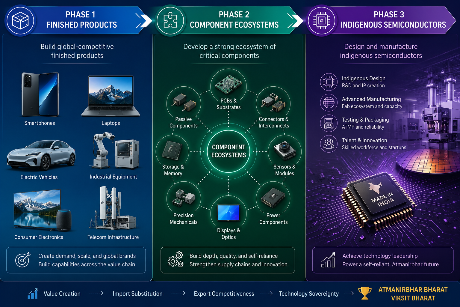
By moving upstream into raw chip packaging, testing, and eventual fabrication, India is capturing the highest-margin segments of global technology manufacturing. The macroeconomic metrics validate this structural overhaul. Since 2014, total domestic electronics production has surged nearly sevenfold, while electronics exports have experienced an astounding elevenfold explosion. The country has safely transitioned into the position of the world’s second-largest mobile manufacturer and exporter, establishing the financial and logistical foundations required to sustain a capillary chip ecosystem.
Sanand is rapidly coalescing into India’s premier chip packaging cluster, mirroring renowned global silicon concentrations like Taiwan’s Hsinchu Science Park or South Korea’s Gyeonggi province. The CG Semi plant follows closely on the heels of major operational milestones from Micron Technology and Kaynes Semicon, transforming the region into an interdependent manufacturing node. When a cluster reaches this critical mass, it triggers a powerful compounding economic effect. Specialized chemical refineries, advanced testing laboratories, precision tool servicing firms, and design startups naturally orient around the cluster, generating thousands of high-value downstream employment opportunities.
Inclusive Growth and Global Investment Stability
A particularly striking dimension of the Sanand industrial rollout is its deep emphasis on demographic inclusivity and human capital development. During his facility inspection, Prime Minister Modi interacted extensively with the highly specialized engineering workforce operating the cleanrooms. A significant cohort of this technical workforce comprises young women drawn from rural and tribal communities across states like Jharkhand, Chhattisgarh, and Madhya Pradesh.
Through targeted state-sponsored technical training frameworks, these individuals were upskilled at Industrial Training Institutes (ITIs) and sent for advanced, hands-on semiconductor operations training in Malaysia. This deliberate synthesis of high-technology industrialization with grass-roots socioeconomic mobility ensures that the dividends of India’s technological leap are equitably distributed across the demographic spectrum.
For global technology investors looking to de-risk their highly concentrated East Asian supply chains, the operationalization of these consecutive facilities sends a powerful signal of stability. The Indian state’s policy framework under the India Semiconductor Mission provides unambiguous financial subsidies, covering up to 50% of eligible capital expenditure for approved units. By matching stable, long-term regulatory policies with rapid infrastructural execution and a massive, highly disciplined engineering talent pool, India is positioning its domestic semiconductor ecosystem as an indispensable, resilient alternate hub for the global technology architecture.
To watch a detailed broadcast detailing the technical specifications of this multi-crore asset and see exclusive footage of the plant floor operations, you can view this Inauguration Coverage of the CG Semi OSAT Facility which provides excellent visual context to the scale of the facility.