
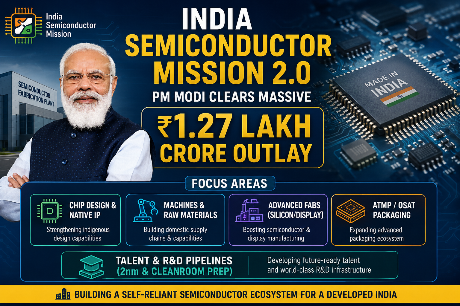
India is spending big money to make its own computer chips. PM Modi and the cabinet just gave the green light to the India Semiconductor Mission 2.0. They are putting Rs 1.27 lakh crore into this new plan. That is way more than the Rs 76,000 crore they spent in the first round. The goal is to make companies feel safe so they can build chip designs and supply chains here.
Before this, India only tried to bring big foreign factories to the country. This new phase changes that strategy. Now, the government does not want just a few scattered factories. They want a complete setup where everything, from the raw chemicals to the final packaging, is done inside India.
Shifting Focus from Raw Assembly to Deep Value Chains
The main change in India Semiconductor Mission 2.0 is its focus on the highly technical, raw supply side of the production cycle. Instead of relying completely on imported chemicals and tools, the government will now give direct incentives to manufacture precision machinery, cleanroom chemicals, ultra-pure gases, and other essential raw materials inside India.
By producing these basic ingredients locally, the government wants to protect the domestic electronics sector from global supply chain delays and geopolitical shocks. The Indian chip market is growing fast, expected to jump from $50 billion to over $100 billion by 2030. To meet this demand, India needs to control the basic raw materials that go into the chips, not just the factories that assemble them.
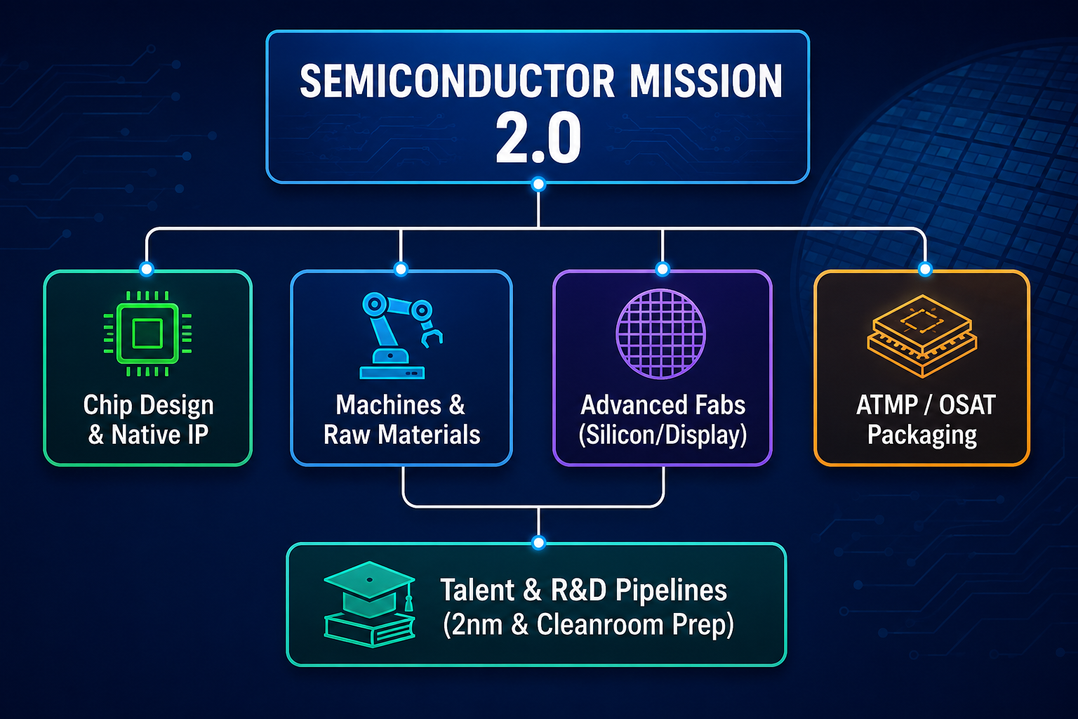
The Six Core Pillars Driving the New Phase
The execution strategy for this expanded phase rests squarely on a structured six-pillar framework, designed to tackle every vulnerability in the electronic production pipeline:
1. Advanced Chip Design and Intellectual Property
Building on early design successes where over 100 startups began actively drafting custom silicon architectures, the focus is now moving toward high-value intellectual property (IP). By identifying specific building blocks for commercial and strategic hardware, the initiative intends to transform the nation into a major global hub for semiconductor design rights and system architectures.
2. Machines and Raw Materials
This pillar lays the foundation for specialized precision engineering. Substantial financial incentives will target companies involved in the research, development, and scaling of semiconductor fabrication machinery. Furthermore, it covers the localized synthesis of complex chemical inputs and gases required inside cleanrooms.
3. Scaling Up Mega Fabs
With the nation’s inaugural commercial fabrication facility firmly on track to be commissioned by 2028, international investor confidence has reached an all-time high. The government will aggressively pitch to global manufacturers to establish additional silicon foundries, compound semiconductor facilities, display fabs, and discrete component plants.
4. Strengthening Packaging Ecosystems (ATMP/OSAT)
Assembly, Testing, Marking, and Packaging (ATMP) alongside Outsourced Semiconductor Assembly and Test (OSAT) units are receiving a massive push. Following initial packaging triumphs, global tech firms are actively viewing India as a primary alternative to traditional East Asian packaging monopolies. The current goal is to bring bleeding-edge, next-generation packaging methods to domestic soil.
5. Forward-Looking Research & Development
While the domestic journey originally took flight using mature nodes ranging between 28nm and 110nm, the tech horizon is shifting. The government is backing advanced R&D projects through structured alliances with elite international and domestic research centers, systematically working toward sub-10nm architectures and eventually aiming for cutting-edge 2-nanometer nodes.
6. Grassroots Talent Development
The human capital engine is already firing, with 315 universities training roughly 68,000 students using industry-standard Electronic Design Automation (EDA) tools. The new phase deepens this academic training by integrating real-world experience, funding specialized cleanroom environments, and training specialized engineers in fab construction techniques.
Reviewing the Solid Infrastructure Built by Phase 1
The sheer scale of the new phase is a direct result of the momentum generated during the initial policy window. The early milestones established a highly functional baseline that proved the region’s operational readiness to the global tech market:
Massive Financial Commitments: Under the initial framework, 12 major chip manufacturing and packaging proposals won official state approval, representing a collective investment pool crossing Rs 1.64 lakh crore.
Diverse Factory Footprint: The approved layout features a highly diversified matrix, consisting of a flagship Silicon Fab, a specialized Silicon Carbide facility, an integrated Gallium Nitride Micro LED Display unit, and nine dedicated packaging hubs. These setups cater directly to fast-growing domestic sectors like automotive electronics, industrial green power systems, aerospace operations, and standard telecommunications.
Active Production Timelines: The ground-level progress is entirely real. Three prominent industry names—Micron, Kaynes Technology, and CG Semi—have transitioned successfully into commercial operations, with another major facility scheduled to fire up production lines within the calendar year.
Incubating Local Innovators: On the software and architecture front, 24 native semiconductor startups and MSMEs secured direct financial backing for their proprietary chip projects, while 105 early-stage entities gained immediate access to professional EDA design suites to prototype custom Systems-on-Chip (SoCs).
“We are witnessing incredibly strong traction and alignment with key strategic partners across the US, Europe, Japan, and Singapore. The government-to-government dialogues, deep industry partnerships, and critical trade discussions are all progressing rapidly to secure a highly resilient global supply chain.” — Ashok Chandak, President of the India Electronics and Semiconductor Association
Long-Term Global and Economic Implications
The impact of this Cabinet clearance goes well beyond basic factory numbers. By offering a stable, long-term policy, the government gives global tech giants the clarity they need to set up multi-year projects and bring in heavy foreign investments.
As international brands try to move their manufacturing away from traditional hubs in East Asia, this new funding comes at the right time. By addressing machinery, chemical engineering, and advanced node research at the same time, the mission makes sure that Indian factories will not get stuck due to global container shortages or raw material embargoes. It secures the supply line for domestic cars, defense equipment, and consumer tech while integrating India into the global tech map.